


By now, we’ve all heard concerning the Synthetic Intelligence (AI) surge that’s going to demand unprecedented quantities of vitality. Even the Worldwide Vitality Company (IEA) launched a report on Vitality and AI just lately. The superior vitality supplies which are the inspiration of those digital options are semiconductors.
Semiconductors and AI Linked by a Extremely Complicated Provide Chain
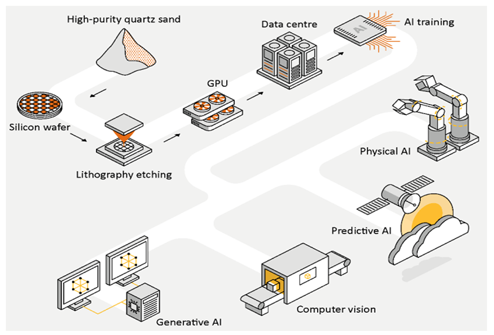
Supply: Worldwide Vitality Company, 2025
What are Semiconductors?
Do you think about that electrical energy flows by way of energy cables like water flowing by way of a pipe? It doesn’t. The electrical energy is all the time there and accessible by way of nodes, e.g., your private home’s energy retailers, which are like gates that open and shut in accordance with while you want energy. Electrons movement freely by way of conducting supplies when these gates are open to ship energy to your electrical car, for instance.
Equally, semiconductors might be regarded as having gates that open and shut, permitting electrons to movement and create circuits. Semiconductors are primarily constructed on silicon, an plentiful and environment friendly materials. These are constructing blocks that type transistors and different parts which are then built-in into complicated circuits on chips. These chips type the core parts that ship computer systems, AI, and different digital options everyone knows.
Semiconductors Allow Cleantech, However Manufacturing Emits Carbon
Regardless of the tiny nature of semiconductors, manufacturing consumes plenty of time, cash, and assets. Constructing a single fab can value upwards of $25B as a result of complicated manufacturing processes which are comprised of tons of of steps, over fifty kinds of gear, and extremely specialised labor. A brand new fab within the U.S. and Europe takes twice as lengthy to design and assemble and prices twice as a lot than in Taiwan.
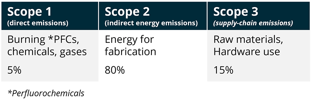
From a sustainability standpoint, manufacturing semiconductors is extremely useful resource intensive. Poisonous ‘endlessly chemical compounds’ (fluorinated chemical compounds/PFAS) make up almost 90% of direct emissions (Scope 1), principally used for cleansing. However changing these chemical compounds may nonetheless be 5-10 years away and non-PFAS alternate options are 20+ years away.
Electrical energy is the only greatest supply of emissions (Scope 2)—60% for manufacturing; 40% for operation of amenities. On the availability aspect (Scope 3 emissions), utilization of recent supplies doesn’t considerably affect the general industrywide emissions profile. Scope 3 emissions are primarily attributed to mining and refining from exterior of the trade. Ahead wanting, world emissions will rise 8% yearly, doubling by 2045 from 2023 (SEMI, BCG, The Semiconductor Local weather Consortium).
Water utilization is one other space of alternative for innovation. Manufacturing a single chip requires 8,327 L of ultra-pure water, and a single fab will devour upwards of 25M-35M L day by day. In Taiwan, fabs will recycle 80% of water utilization, however in most different international locations solely 10% or much less is recycled. From 2021-2024, Micron and Aqua Membranes have been growing expertise to recycle water utilization. After profitable trials, the 2 are dedicated to recycling 95% of Micron’s water utilization by 2030.
Key Improvements – Design, Photonics, and Compound Supplies
No single breakthrough innovation is catapulting the trade ahead from a sustainability standpoint, however there are a variety of thrilling areas to concentrate to.
Design – Mental Property (IP) Reuse
IP reuse and discovery is primarily completed manually by engineers, however digital options are coming on-line breaking by way of the traditionally cost-prohibitive boundaries that stored many fabs from uptake.
![]()
Thalia is a supplier of a software program platform that permits semiconductor companies to develop new merchandise utilizing current chip designs for analog. Thalia leverages AI/ML to mine information for IP reuse to streamline design to fabrication. This automation results in diminished cycle time and prices for its clients and in the end improved element reliability.
Design – Supplies
The person wafers could also be designed with compounds like gallium nitride or indium phosphide. These could have effectivity will increase and should lead to carbon emissions reductions at smaller scales.
PseudolithIC is a producer of hybrid semiconductor merchandise which combine compound semiconductor chiplets into silicon wafers. These compound chiplets mix the vitality capability of excessive vitality supplies (compound III-V) like gallium, indium, and so on., with silicon. This maximizes efficiency whereas decreasing manufacturing prices. It’s concentrating on the RF market with protection and telecom markets main in demand.
Fabrication – Photonic Built-in Circuits (PICs)
PICs use mild (photons) moderately than electrical energy to course of data. This interprets into vitality waste discount for quicker and extra environment friendly information dealing with. Whereas not projected to scale within the 2030s, PICs do symbolize important vitality financial savings potential. It’s thought that PICs will have an effect just like the microelectronics revolution within the Eighties. PICs may ship merchandise which are an order of magnitude quicker than right now’s electronics.
![]() NXP Semiconductor backed Sensible Photonics is a producer of indium phosphide (InP) semiconductors for PICs. Sensible Photonics just lately partnered with X-Fab and Epiphany Design to reveal InP-on-Silicon for optical transceivers. It intends to focus on datacenters, sensing, and telecom.
NXP Semiconductor backed Sensible Photonics is a producer of indium phosphide (InP) semiconductors for PICs. Sensible Photonics just lately partnered with X-Fab and Epiphany Design to reveal InP-on-Silicon for optical transceivers. It intends to focus on datacenters, sensing, and telecom.
Metrology
High quality management, course of optimization, and testing software program and gear maintain contaminates out for prime precision manufacturing.
![]() Wooptix is a producer of semiconductor metrology gear incorporating wavefront part imaging (optics) for non-invasive sensing to make sure that every element meets stringent high quality requirements.
Wooptix is a producer of semiconductor metrology gear incorporating wavefront part imaging (optics) for non-invasive sensing to make sure that every element meets stringent high quality requirements.
![]() K2 Photonics developed a single cavity dual-comb laser for metrology for semiconductor inspection. This supplies fast and exact thin-film inspection.
K2 Photonics developed a single cavity dual-comb laser for metrology for semiconductor inspection. This supplies fast and exact thin-film inspection.
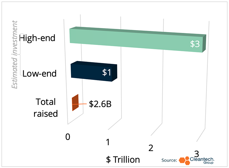
$2.6B Whole VC Funding for Semiconductors from 2020-2024:
Removed from $1T-$3T Wanted by 2030
Geopolitical Tensions, Rising Prices, Undeveloped Provide Chains
The chance to bolster AI and datacenters, amongst many different cleantech purposes, is threatened by the semiconductor trade’s focus in Taiwan. Vulnerabilities throughout the provide chain are additional exacerbated by geopolitical tensions just like the U.S.’ 32% tariffs imposed on exports from Taiwan. We’ve seen important funding by the general public sector just like the $53B U.S. Chips & Science Act or the $47B EU Chips Act.
However these investments haven’t resulted in any important breakthrough technological developments but, particularly in Europe and China. International locations are pressuring incumbents to develop enterprise exterior of Taiwan, however incumbents are pushing again, calling on policymakers to offer monetary incentives, e.g., subsidies for supplies. Nonetheless, the present mission pipeline is booming, notably for the U.S. that has dedicated over $540B in provide chain investments since 2020 by way of grants, loans and mission growth:
- TSMC has invested $165B to construct new fabs within the U.S.
_ - Nvidia introduced a $500B plan to fabricate in Arizona in partnership with TSMC and plans to construct out extra fabs in Texas with Foxconn and Wistron
_ - Apple is about to take a position over $500B to construct new fabs in U.S., as nicely
From 2020-2024, we tracked over $2.6B of VC investments for semiconductor innovation. That is removed from the estimated $1T-$3T price of funding wanted from 2020-2030 in R&D and capital to ship the following technology of semiconductors (The Semiconductor Trade Affiliation, BCG). These figures are estimated for the semiconductor trade as a complete, not simply cleantech. We spent roughly this a lot to get us the place we’re right now, so these figures, whereas giant, are manageable.
A part of the explanation for these giant figures is the associated fee to construct a semiconductor fab and its extremely complicated provide chain. Resulting from this complexity, no single producer nation is able to manufacturing semiconductors with out sourcing some a part of the availability chain from elsewhere. This presents an particularly profitable alternative for play on this distributed provide chain to permit for faster lead occasions and higher collaboration among the many ecosystem.
